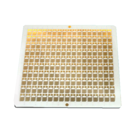
DPC technology (Direct Plated Copper)

DPC is one of the technologies used in the world to form a topology of various thicknesses.
Due to the excellent resolution, DPC technology allows you to achieve high density packaging topology. The topology resolution is determined by the required thickness of the copper metallization. The ratio of the width and thickness of the conductor is 3:1. With a metallization thickness of 20 microns, the minimum width of the conductor is only 60 microns.
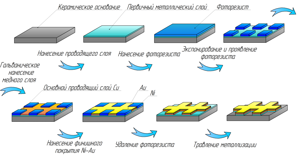
One of the distinctive features of this method is the possibility of forming a vertical side wall of the conductor, which is extremely difficult with thick-film technology. The figure shows one of the variants of this technology.

Stapes of the technological process:
1. Formation of a thin continuous film of conductive material on a ceramic substrate. In this case, there may be holes in the substrate;
2. Applying a photoresist to the formed conductive layer;
3. Exposure and manifestation of photoresist;
4. Galvanic build-up of copper metallization of the required thickness;
5. Application of Ni-Au finish coating;
6. Removing the photoresist from the surface of the board;
7. Chemical etching of the conductive layer remaining on the ceramic after removing the photoresist.
Specifications

|
Properties |
Thick-film technology |
DPC |
|
Tolerance |
± 10% |
± 1% |
|
Adhesion |
high |
high |
|
Surface roughness Ra, mkm |
от 1 до 3 |
≤ 0,3 |
| Pages |

|

|
Technology comparance (the 5 - the best items, the 1 - the lowest items)
|
Properties |
DPC |
Thin- film technology |
Thick-film technology |
|
Electrical conductivity |
5 |
3 |
4 |
|
Thermal conductivity |
5 |
3 |
4 |
|
Stability of parameters |
5 |
5 |
3 |
|
Resolution |
4..5 (определяется толщиной медного слоя) |
5 |
2 |
|
Cost |
5 |
2 |
2 |
| Ceramics |
Thickness, mkm |
Conductive material of the transition holes |
Tolerance for the width of the conductor, microns |
||
|
Cu |
Ni |
Au |
|||
|
Al2O3 |
1... 100 |
3 ... 5 |
0,075... 1 |
Ag, Cu |
50 |
|
AlN |
|||||
An equally important characteristic that determines the durability of products is the resistance of the metallized board to temperature effects. Thermal cycling testing was carried out according to MIL-STD-202.107G. This method is designed to determine the stability of a ceramic substrate with metallization to a cyclic temperature change.
Test conditions:
- -400C (30 min)~1250 oC (30 min), 500 cycles;
- adhesion measurement method: bursting machine;
- conditions: adhesion ≥ 3 kg.
Test results
|
№ |
Value, кг |
Results |
№ |
Value, кг |
Results |
|
1 |
3,84 |
+ |
6 |
3,94 |
+ |
|
2 |
3,92 |
+ |
7 |
4,11 |
+ |
|
3 |
4,02 |
+ |
8 |
3,51 |
+ |
|
4 |
3,76 |
+ |
9 |
3,87 |
+ |
|
5 |
3,58 |
+ |
10 |
4,01 |
+ |
|
Average adhesion value, кг: 3,86 ± 0,18 |
|||||
Application area
- solar collectors;
- power electronics:
- power integrated circuits;
- thermoelectric coolers and generators;
- microwave appliances;
- Microwave devices;
- LED leds.