Подложки DBC (Direct Bonded Copper)
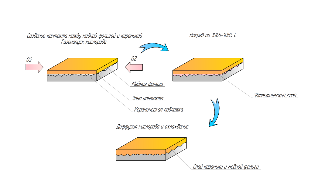
The DBC (Direct Bond Copper) technology consists in attaching a thick copper foil with a thickness of 0.125 to 0.700 mm to a ceramic substrate based on aluminum oxide or nitride. High adhesion rates are provided due to eutectic coupling and mutual diffusion of oxygen molecules in the contact zone of copper with ceramics.
DBC technology allows you to create boards with a topological pattern similar to the etching technology of printed circuit boards, while thick copper conductors provide excellent current conductivity and heat dissipation from semiconductor power crystals, which is necessary for effective cooling of power supply components.
DBC substrates can operate in the temperature range from -100 to 250°C, have the ability to withstand higher currents compared to other metallization methods, such as screen printing or electrochemical coating, and provide higher voltage isolation (up to several thousand volts).
Also, the technology allows you to get boards with transition holes.


DBC technology steps:
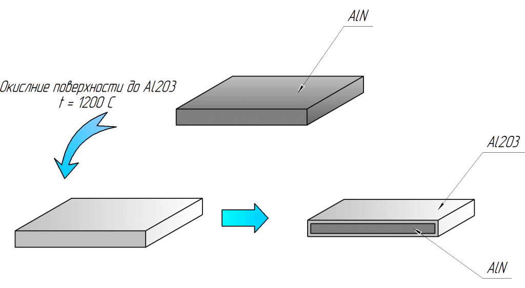
1. Transformation of the ceramic surface due to its oxidation. This step is necessary exclusively for aluminum nitride;
2. Bringing the copper foil into contact with the ceramic substrate;
3. Sintering of copper foil with ceramic substrate in special furnaces with controlled oxygen levels. Oxygen diffusion occurs in the contact zone and the formation of a thin binder layer of foil and ceramics.
The technology of manufacturing boards using DBC technology consists of the following stages:
1. Sintering of copper foil and ceramic substrate;
2. Applying a resistance;
3. Exposure and manifestation of resistance;
4. Chemical etching of the topological pattern;
5. Laser scribing;
6. Final etching of copper;
7. Removing the resistance layer;
8. Formation of the finishing coating. As a finishing coating, layers of chemical nickel and gold, HASL, etc. are used.
Specifications

|
Properties |
Value |
|
The content of the main substance, % |
99,00 |
|
Static bending strength, МПа |
193,90 |
|
Specific volumetric electrical resistance ( 25 оС), Ом•см |
40,00 ∙ 1014 |
|
Loss angle tangent (8-10 ГГц) |
1,50 ∙ 10-4 |
|
Dielectric constant ( 8-10 ГГц) |
7,30 |
Coefficient of thermal expansion (∙ 10-7 1/оС) |
|
|
20 - 200 |
59,00 |
|
20 - 500 |
70,00 |
|
20 - 900 |
77,00 |
|
20 - 1000 |
80,00 |
|
Porosity, % |
0,07 |
|
Thermal conductivity (при 20 оС), W/м ∙ град |
21,00 |
|
Equivalent thermal conductivity, W/м ∙ С |
209,50 |
|
Breakdown voltage, кV |
15,00 |
Characteristics of conductive tracks
|
Copper thickness, мм |
Distance between conductors, мм |
Width of conductors, мм | ||
|
Тип. |
Мин. |
Тип. |
Мин | |
|
0,127 |
0,30 |
0,25 |
0,30 |
0,25 |
|
0,20 |
0,50 |
0,40 |
0,50 |
0,40 |
|
0,25 |
0,60 |
0,50 |
0,60 |
0,50 |
|
0,30 |
0,70 |
0,50 |
0,70 |
0,50 |
|
0,40 |
0,80 |
0,60 |
0,80 |
0,60 |
|
0,50 |
0,90 |
0,70 |
0,90 |
0,70 |
Using ceramics
|
Properties |
Description |
|
Material |
Al2O3 (96%), AlN |
|
Maximum size, мм |
138 х 188 |
|
Thickness, мм |
0,25; 0,38; 0,5; 0,635; 0,76; 1 |
|
Loss tangent (250 oС/1 МГц) |
≤ 3 ∙ 10-4 |
|
Thermal conductivity W/(м ∙ K) |
> 24 |
|
Dielectric strength |
> 14 |
|
Dielectric constant (250oС/1МГц) |
≤ 9,4 |
Ceramics-conductor
For Al2O3
|
Ceramic thickness, мкм |
Cu thickness, мкм | ||||
|
0,127 |
0,20 |
0,25 |
0,30 |
0,40 | |
|
0,25 |
✔ |
✔ |
✔ |
- |
- |
|
0,32 |
✔ |
✔ |
✔ |
✔ |
- |
|
0,38 |
✔ |
✔ |
✔ |
✔ |
- |
|
0,50 |
✔ |
✔ |
✔ |
✔ |
✔ |
|
0,63 |
✔ |
✔ |
✔ |
✔ |
✔ |
|
0,76 |
✔ |
✔ |
✔ |
✔ |
✔ |
|
1,00 |
✔ |
✔ |
✔ |
✔ |
✔ |
For AlN
Ceramic thickness, мкм |
Cu thickness, мкм | |||||
|
0,127 |
0,20 |
0,25 |
0,30 |
0,40 |
0,50 | |
|
0,25 |
✔ |
✔ |
✔ |
✔ |
- |
- |
|
0,38 |
✔ |
✔ |
✔ |
✔ |
- |
- |
|
0,63 |
✔ |
✔ |
✔ |
✔ |
✔ |
✔ |
|
1,00 |
✔ |
✔ |
✔ |
✔ |
✔ |
✔ |
Conductor's properties
|
Properties |
Value |
|
Thermal conductivity W/(м•K) |
385 |
|
Thickness, мм |
0,07 – 0,4...0,3±0,015 |
|
Chemical composition, % |
99,99 |
|
Separation force, N/мм |
>6 |
|
Operating temperature, ℃ |
от -55 до +850 |
|
Surface roughness Ra, мкм |
≤ 3 |
|
Etching defects, мкм |
≤ 30 |
Application area
- thermoelectric modules and Peltier elements;
- power integrated circuits;
- Microwave devices;
- electric locomotive power engines;
- medical equipment;
- various high-power semiconductor devices and their packaging;
- car electronics;
- other products.