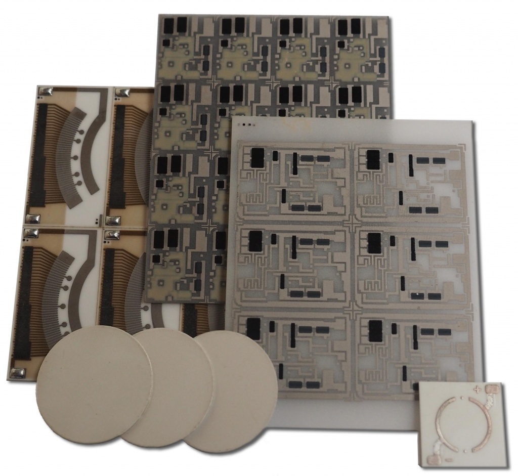
Thick-film technology
 Thick-film technology is a fairly common technology for applying thick layers for various purposes, due to the sintering of special pastes with a ceramic substrate. It is a very cheap and productive method that allows to obtain reproducible thick layers (from 8 microns) for various purposes.
The technological process consists of the following stages:
- Application of a special paste on a ceramic substrate;
- Heat treatment of paste;
- Applying a protective layer.
Heat treatment includes drying to remove the solvent from the paste and directly burning the paste into the ceramics. The protective layer is not applied for GIS installed in the housing. As a protective layer, glasses with a low softening temperature (no more than 500C) are used.
Specifications

|
Properties |
Value |
|
Resolution (conductor/gap), microns |
от 44 до 200 |
|
Ceramics used |
Al2O3 (ВК-94, ВК-96), AlN, BeO и etc |
|
Pastes used |
resistive, conductive, dielectric, polymer (protective) |
|
Metallization thickness, mkm |
от 8 до 100 |
Application area
-
thick - film GIS;
-
magnetic bearings.
-
solid-state relays;
-
thermoelectric modules;
-
various inductors;
-
ionizing radiation sensors;
-
sensors for liquid level, pressure, position, etc.;
-
solar collectors;
-
thick-film active and passive elements